

产品中心
Product Center
Graphene
Category
Product accessories
The ideal graphene structure can be regarded as exfoliated monoatomic layer graphite. The basic structure is a two-dimensional crystal material with six-membered ring benzene units and infinite expansion. This is currently the thinnest material in the world - a material with a thickness of one atom. . This special structure contains rich and novel physical phenomena, which makes graphene exhibit many excellent properties.
Product details
The ideal graphene structure can be regarded as exfoliated monoatomic layer graphite. The basic structure is a two-dimensional crystal material with six-membered ring benzene units and infinite expansion. This is currently the thinnest material in the world - a material with a thickness of one atom. . This special structure contains rich and novel physical phenomena, which makes graphene exhibit many excellent properties.
Characteristic
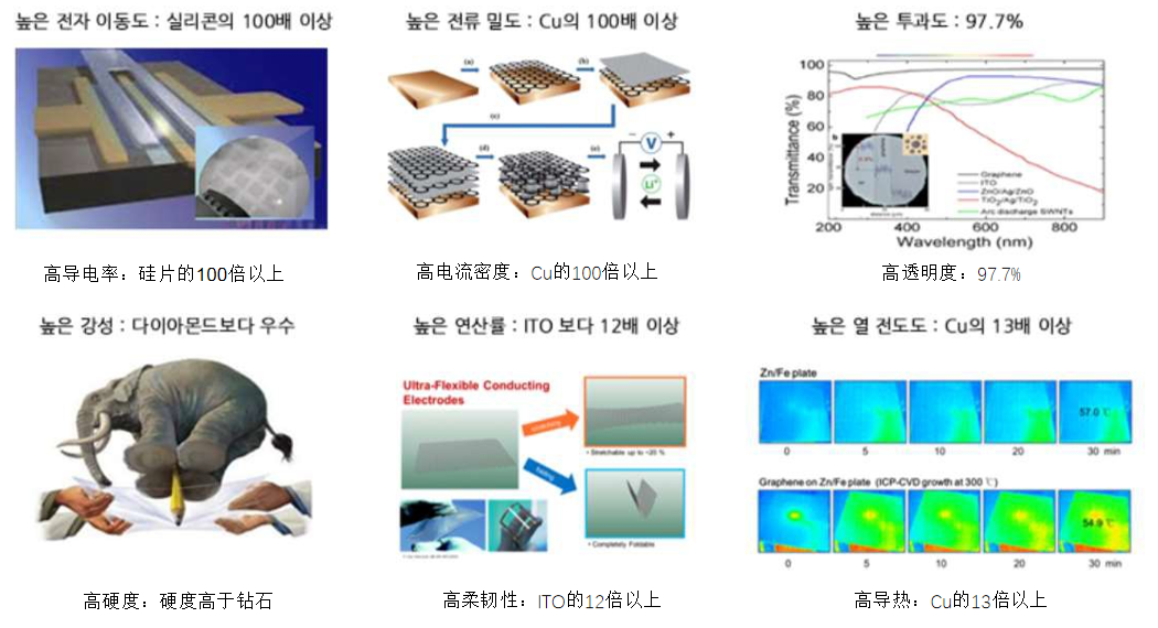
Unique properties
| Classification | Performance | Performance description | Application field |
| "Most" performance | The softest | Mohs hardness is only 1~2 | Flexible Electronics |
| The thinnest | Thickness of 0.335nm, 1/200,000th of a hair | Nanoelectronic devices | |
| Highest intensity | Tensile strength 130MPa, Young's modulus 1TPa | Composite material | |
| Fastest electron transport | Carrier mobility 15000cm2/V s (10 times that of silicon material) | Sensing, display, energy storage | |
| Fastest heat transfer | Thermal conductivity 5000W/(m·K) | Heat conduction, heat dissipation material | |
| "Special" performance | Translucency | The single layer is almost completely transparent, and the absorbance increases linearly with the number of layers | Optoelectronic devices |
| Flat crystal | Excellent crystal structure properties | - | |
| Large specific surface area | Specific surface area 2630m2/g | Sensing, Display, Energy storage | |
| Room temperature ferromagnetic effect | - | Microelectronics, Memory Chips |
Preparation
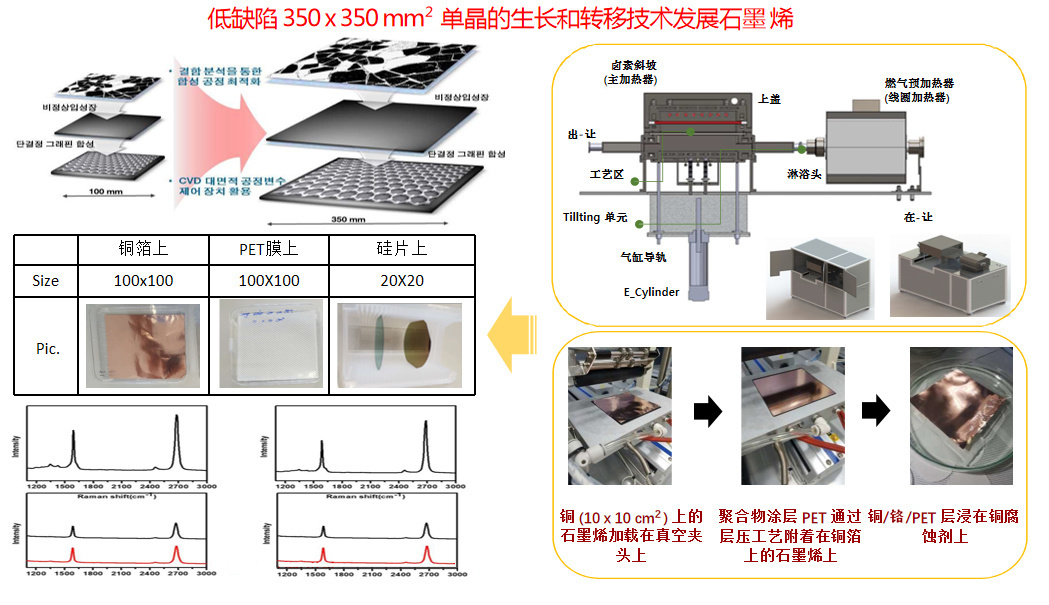
1.1 Brief description of Thermal CVD method
The preparation of graphene by chemical vapor deposition (CVD) generally selects CH4, Ar, H2 and other gases as precursors, and transition metal crystals as substrates. Put the metal substrate in a closed container (such as a quartz tube), and the carbon atoms generated by the high-temperature catalytic cracking gas are deposited on the surface of the transition metal to form a graphene film. This method can prepare a large-area graphene film, but the required The temperature is high, the size of the grown graphene is limited by the substrate, and the substrate needs to be removed, which is costly. In the preparation process, with the assistance of plasma, the grown graphene will have better crystallinity, fewer defects, and fewer layers (about 5 layers), so the quality is higher.
1.2 The CVD method is the most potential method for large-scale, high-quality, and large-size graphene film preparation.
There are two main principles of common chemical vapor deposition methods:
Carburization and carburization mechanism: For metal substrates such as Ni with a relatively high dissolved C content, the carbon atoms produced by the cracking of carbon sources infiltrate at high temperatures, and when the temperature decreases, they are precipitated from the substrate to nucleate and grow into graphene
Surface growth mechanism: For metal substrates such as copper with low dissolved C content, at high temperature, the gaseous carbon source is cracked to generate carbon atoms that adsorb on the surface, grow into graphene islands, and then grow two-dimensionally and merge to obtain graphene.
CVD Equipment and Development Status
Application fields and development goals
Touchscreens, folding screens, foldable OLEDs, photodetectors, biosensors, modulators, semiconductors, spin-troic sensors, spin-optic hybrids, wave generators, logic transistors, radio-frequency-transistors, wave detectors;
Thermal diffusion plates, flexible displays, automotive heaters, barrier films, biosensors;
Related products


Contact us
Address: Building 37, Longhu Science and Technology Innovation Park, Longzihu District, Bengbu City, Anhui Province
WeChat sweep